
simmconn
-
Posts
173 -
Joined
-
Last visited
-
Days Won
2
Content Type
Profiles
Forums
Events
Everything posted by simmconn
-
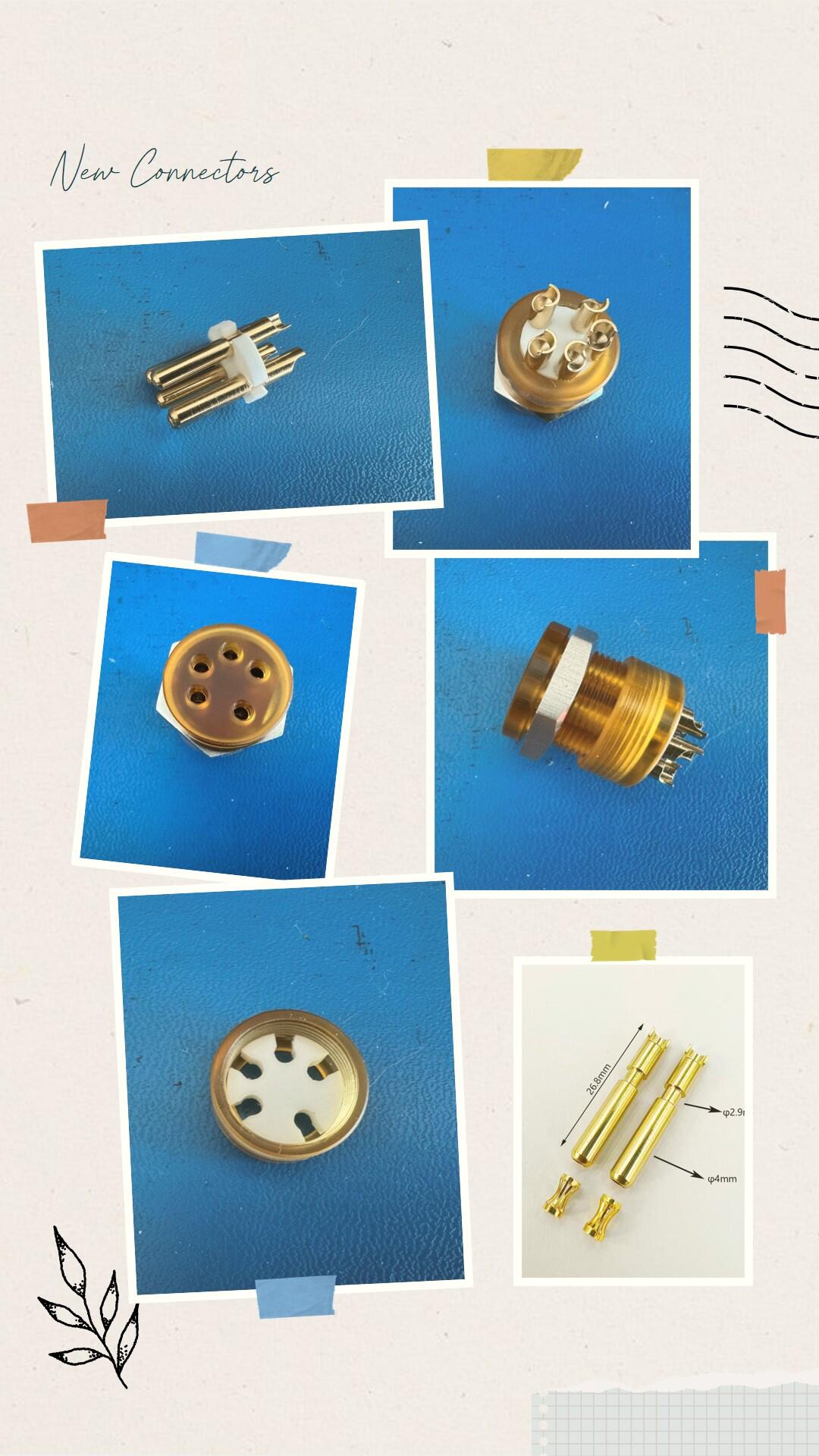
I found a 2.3mm receptacle contact with a lantern-type spring insert, which should be able to tolerate some radial misalignment without too much change in the mating force. I've been toying with the idea of a multi-part jack. The pin center diameter was chosen to be 10.75mm in order to accommodate the Stax, the Hifiman and the less accurate Kaldas plug with the acrylic base. The contact retainer washer is made from Teflon which also gives a bit of flexibility. The connector and shell can be made from PEEK but I can't help trying the PEI (Ultem). Its translucent color matches with the gold plated contacts quite well. There are two variations of the design, with the retainer sandwiched between the shell and the cap, and with the retainer secured flush with the cap. The latter requires better precision from machining.

-
and now for something completely different part 3
simmconn replied to kevin gilmore's topic in Do It Yourself
I don’t see how the bias servo could have worked. You have the + input of the opamp connected to the amp output terminal, which means the integrator has a dancing reference that it has no rejection of. Furthermore, a divided down version of that amp output signal is shared with other servos, an interesting way to create crosstalk? -
I was just pointing out, as how Q12 is connected today, it’s not doing what it is supposed to do. The output should be connected to gate instead. I remember last time you recommended TTC004B as a replacement for the PZTA42 (different package). We just need something with a flat hfe-Ic curve to, say >100ma at VCE=10V.
-
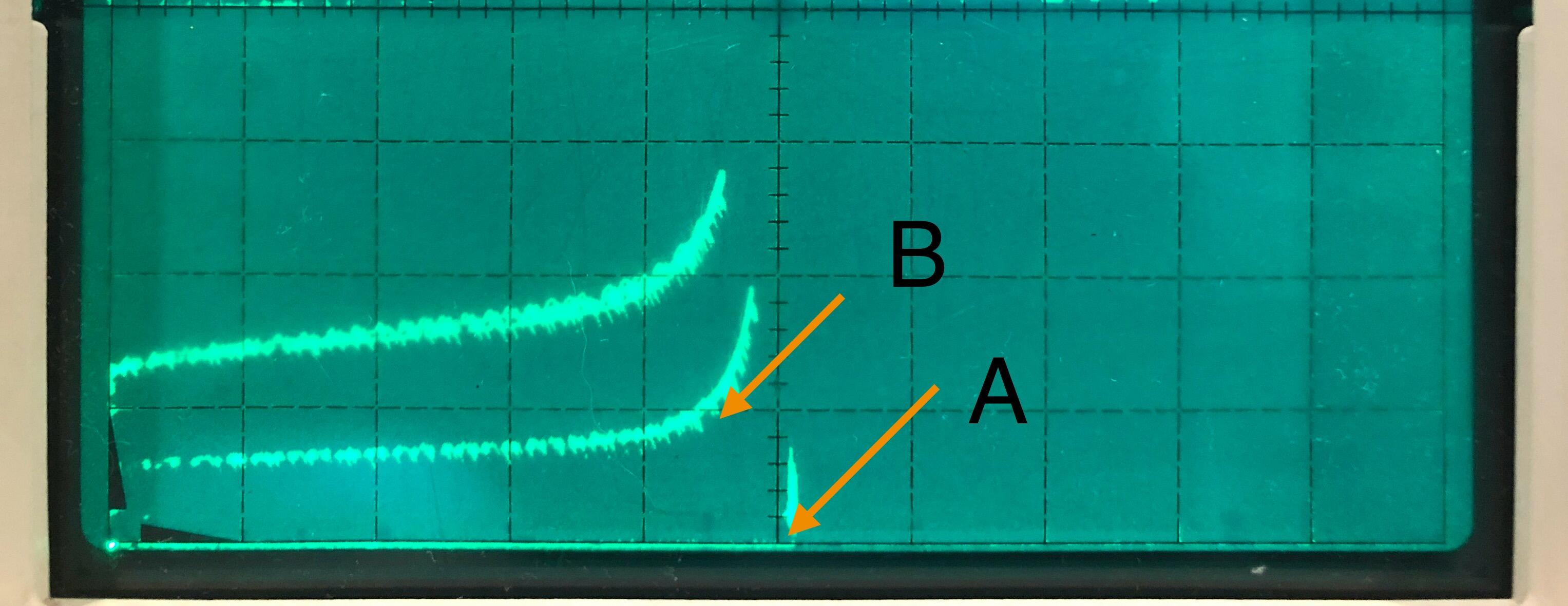
Q12 in the PSU seems full-on and not doing much if anything. I noticed that the 2N3904-based current limiter is not there. Many people say it is too slow, not realizing that it is protecting the passing SiCFET at every power up, before the opto coupler soft start switch is released. On the other hand, if the SiCFET decides to give up, nothing can hold it back anyways. The 2N3904-based current limiter should not be the one to blame. The amp section still uses PZTA42 despite the linearity issue we found earlier and better options are available. The STN9360 although is specified with a 600V VCEO, its curve shows onset of breakdown at a lower voltage. I didn’t take a picture with the STN9360, but the one below is similar. Technically the breakdown voltage is specified at point A, but you wouldn’t want to operate the part at point B, even though that’s still “within spec”.
-
Megatron Electrostatic Headphone Amplifier
simmconn replied to kevin gilmore's topic in Do It Yourself
Adjust R31 or R32 for 2.5V, and then adjust R33 or R34 for 5V. They should be independent as long as you do it in that order. Take into account of the wire resistance when measuring voltage especially in the 2.5A case, when you get into mV of accuracy. -
Megatron Electrostatic Headphone Amplifier
simmconn replied to kevin gilmore's topic in Do It Yourself
A lot of those filament regulators focus on reducing the differential mode noise. I think the DHT would be more sensitive to common mode noise, because the filament itself is the cathode in the signal path. Depending on the circuit topology, you may or may not be able to bypass the noise to ground. The common mode noise starts from the secondary windings on the power transformer, and gets more complicated with the switching regulators noise riding on top of it. It depends more on the implementation than the pretty numbers in the datasheet. -
Megatron Electrostatic Headphone Amplifier
simmconn replied to kevin gilmore's topic in Do It Yourself
It’s a pretty ingenious design. It takes advantage of the fact that a cold filament draws more current than when it’s hot and thermally stable. The circuit outputs 2.5V by default at no load in case someone does a hot-plugging. An 2A3 draws more current than 2.5A when cold, and gradually drops down to 2.5A. The output is maintained at 2.5V. If it’s a 300B instead, the current would drop further, say, below 1.6A. The circuit would then switch to 5V, and the threshold also doubles to 3.2A. There could be some brief back and forth, but as the filament gets hotter, the current will drop further towards 1.2A while the circuit stays at 5V output. It should be okay for a DIYer to build a clone for his/her own use, but integrating the same in a “DIY” unit that sells for an atrocious price at “the marketplace” would probably be a different matter. -
Megatron Electrostatic Headphone Amplifier
simmconn replied to kevin gilmore's topic in Do It Yourself
Looking at the CTR curve I would choose the operating range between 1 to 2mA of If. Since the nominal CTR is 20%, the phototransistor side would be designed around 200uA to 400uA. Adjust the resistors such that the desired normal bias voltage is centered around this range. The phototransistor could operate off the 110V supply if you don’t need the full 510V range for the bias adjustment (why would you?). -
I can contribute two data points. Out of the two X9000 era Stax plugs I measured, the pin diameter is within 2.36+/-0.004mm, and the pin circle diameter is about 10.95mm. The pins are not perfectly parallel to each other, and the pin circle diameter is slightly larger at the tips.
-
Megatron Electrostatic Headphone Amplifier
simmconn replied to kevin gilmore's topic in Do It Yourself
Interesting design! I’d be a bit worried about the thermal and mechanical side of things. The thermal resistance of the heatsink this size is probably going to run above 5C/W without forced air flow. It is going to run too hot to touch at 350V to 400V/20mA (7 to 8W). With 3C/W theta JC on the 10M90S, there is still margin on the die temperature. If I were to design a PCB to be plugged into a tube socket with soldered pins, I’d use slightly undersized pins and whatever copper I can get for adhesion to the board (double layered board with plated-thought holes in 2-mm or thicker PCB), especially if the counterpart is the unforgiving “modern” tube sockets with tulip type spring contacts. Last but not least, when the whole thing gets very warm, I’d use materials with higher working temperature such as ASA or ABS. PLA is probably not going to last very long. -
I guess the machine shop cheaped out and didn’t use 5-axis tool paths for those steep facets. Otherwise we wouldn’t see the tool marks after heavy sandblasting. This should really have been a cast part. No objections from the environmentalists from the other side of the pond? I’m surprised.
-
Thanks. I guess nobody likes to receive fake parts. But if it’s a low-current, 1200V or better grade IGBT, its characteristics can come very close to the SiCFET we use in threshold voltage, transconductance and even input/output capacitance. It might actually work, at least in the GRHV. I’d be interested to try it out. Well, we should probably stop talking about SicFET or IGBTin this thread, as they are irrelevant to T2.
-
You haven’t answered my question how you determined that the part is a fake (other than from the appearance).
-
If you use them in a constant current source, the Vbe-Ic curve (figure 10) is probably more important than hFE. If you don’t have ways to measure, pick two that are closest in hFE for each channel and hopefully they come close in other parameters as well. If you ask me, I always order at least 2x more than the BOM qty and match them on a curve tracer at or near the actual operating point. The bigger the pool, the more likely you’ll end up with well matched pairs.
-
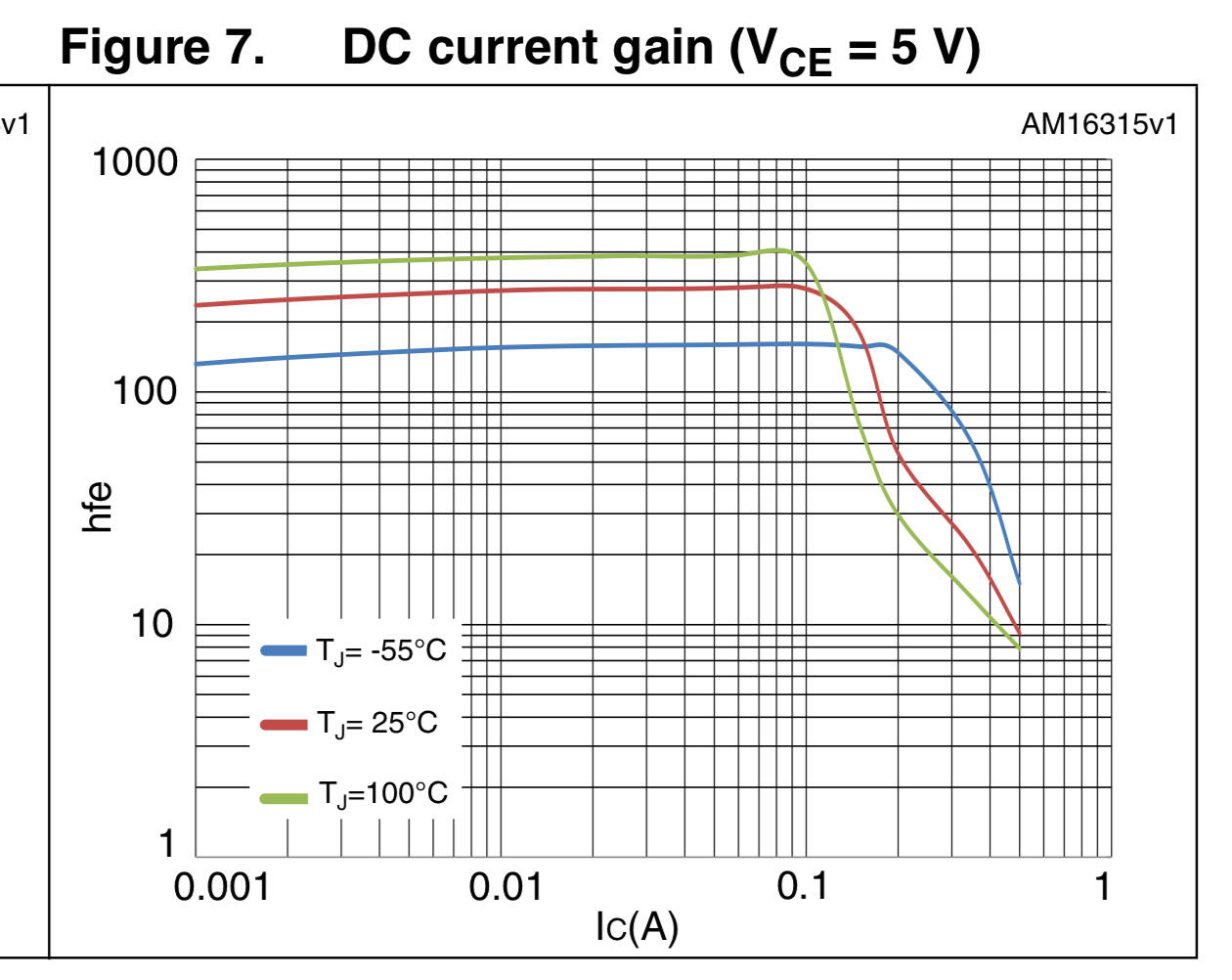
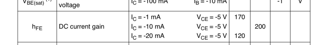
If I were to choose from a well executed raster image logo in the marking and a badly burned vector one, I’d opt for the latter in a heartbeat. I’ve explained the reason and would not repeat here. For the hFE, you need to know the Ic and Vce your testing was performed at, in order to make a meaningful comparison with the numbers in the datasheet. If you don’t know, measure them. The datasheet says minimum hFE is 170 at 25 degree C, Ic=-1ma and Vce=-5V. From the chart you can see hFE goes slightly up from Ic=-1ma to -10ma and then to -20ma before it starts to drop after Ic=100ma (the red line). If your sample tests at hFE=150 between Ic=-1ma and -10ma, it’s below spec and would be a reject by the factory. You can see the red line is well above 200 and approaching the 300 line, so 340 is not a surprise. +/-20% is considered normal variation. Why would they specify min hFE at only 120 at Ic=-20ma? It could be a simple mistake, or indicating that the hFE could drop as early as Ic=-20ma, unlike what the typical curve suggests, which is a bad news for circuit designers (not applicable for our applications). Nevertheless, sandbagging would not get them into trouble anyways, if you know what I mean. I could go on and on and brag about my affiliation with the semiconductor industry, but let’s keep the personal information out of this discussion. If you think my comments make sense, think about it. Otherwise, just take it with a grain of salt.
-
How do you determine if a part is a fake? If a part with a poorly done or a suspiciously looking marking meets all the specifications of the genuine part that you can verify, would you still declare it a fake?
-
Okay. Please do report back when you hear from Mouser, then I’ll explain why I think hFE of 341 is more reasonable than 150 for an STN9360.
-
You offered your opinion and analysis, I offered mine. Although we disagree, I hope we can respectfully disagree.
-
Mouser is legit, ‘Mauser’ is probably not. The one in the first picture is more likely a fake. Even without a known genuine sample for comparison, you can tell by at least two factors: The four top corners of the plastic molding are rounded and inconsistent, suggesting that the package may have been sanded. The ST logo is a raster image composed of parallel horizontal lines, suggesting that it is a scanned reproduction. A genuine product would have a vector artwork since it is the manufacturer’s original design. Other factors such as the laser marking font or etching depth can vary from manufacturer from manufacturer and even from factory to factory. You would need a known genuine sample for comparison. A low cost transistor tester such as DY294 can test breakdown voltages up to 1kV and measure hFE at different collector current settings. You can choose one that’s close to the transistors’ actual operating point. DY294 Digital Transistor DC Parameter Tester Field Effect Tube Tester Multifunction Semiconductor Tester https://a.aliexpress.com/_mqGVojt
-
Picture 2: An “audio grade transformer “ didn’t care to color code the wires properly, such that the assembly tech has to attach hand-written labels to tell them apart. Maybe only the decal is custom made? Nonetheless it shows the production volume of this kit. Picture 3 and 4: It’s funny they try to use different colored quick disconnect to do dummy-proofing. Did they not know that those quick disconnects are colored differently for a reason? Pink/red for 18GA or smaller, blue for 14/16GA and yellow for 12/10GA. They used similar wire sizes regardless of the requirement of the quick disconnect, and the yellow one is apparently oversized (loose crimping). So much for a “professionally put together” kit.
-
Megatron Electrostatic Headphone Amplifier
simmconn replied to kevin gilmore's topic in Do It Yourself
It’s not hard to do a 1:1 clone of the PCB. It’s also a great interview question for a junior electrical engineer to come up with a circuit that does this. However not a lot of them would probably know how a vacuum tube filament/heater behaves. -
There are plenty of suitable candidates for the SiCFET. I count 9 different parts just by running a simple search on Digikey. Look for 1700V rated Vdss, IDmax less than 10A, Ciss less than 240pf, TO-247-3 package. I would prefer ones that are DC-SoA rated, with a moderate transconductance, low and stable Crss across the entire VDS range. Avoid those that are not characterized for linear operation. The vendor doesn’t want to guarantee those use case, and you will be on your own. I would try the onsemi NVHL1000N170M1 if I were to build another KGSSHV Carbon, although there are cheaper options that may be as good. The closest sub for LT1021 is the LT1236. As far as I know they only differ in long-term drift specs. There are other shunt mode 10V references but none come close to the noise performance of LT1021/LT1236. Of course you can also use second-hand, recycled ones. Those are cheap and already aged to perfection (in terms of long term drift).
-
Megatron Electrostatic Headphone Amplifier
simmconn replied to kevin gilmore's topic in Do It Yourself
Ok, I stand corrected. The Megatron XL uses a 'hybrid' biasing scheme for the 300B. The grid is adjustable between 0 and 0.99% of B- ('fixed'-biasing), which cancels out less than 10% of the bias generated by the cathode resistor (self-biasing). The voltage between the cathode (K) and the grid (G) is the actual grid bias (Vgk), regardless of self-bias or fixed-bias. In a fixed bias setup, you’d measure between GND and G when K is grounded. -
Megatron Electrostatic Headphone Amplifier
simmconn replied to kevin gilmore's topic in Do It Yourself
The Megatron final stage is CCS-loaded single-ended output working in class-A. There is no problem selecting operating point that way. However the final stage is self-biased. The grid bias eats up part of the B-, in other words B- is not equal to Eb in the tube datasheet. 20 to 30mA is more than enough for an estat amp. Since 300B has a low mu (2.85), which is about 1/3 to 1/4 of a triode-strapped EL34, the undistorted output voltage will be less than with EL34. But the DHT fame and the aesthetics probably more than compensate for that. -
Not exactly the same part but being the same package they are more in common that they are different: https://fscdn.rohm.com/en/products/databook/applinote/ic/power/linear_regulator/to252_thermal_resistance_information_an-e.pdf In the final stage CCS, the 10M90S is dissipating 8W to 9W. The theta-JA needs to get down to single digit °C/W in order for the junction to stay comfortably within spec, not to mention that the output DC offset thermal drift has always been our enemy. TO-252 is not going to get you there. Also, even if the copper is well coupled with the aluminum angle, the tiny cross section would still give considerable thermal resistance. You are right in that it is just like the Ohm's law. With theta-JC being 3.1 already, there is not a lot of slack to play with. I think IXYS is being sloppy when it comes to thermal specs in the 10M90S datasheet, by specifying only one number for both packages. With some other parts having about 2x theta-JC in TO-252 than in TO-220, I doubt IXYS can do that much better.