Leaderboard
Popular Content
Showing content with the highest reputation on 11/25/2024 in all areas
-
5 points
-
4 points
-
3 points
-
3 points
-
Unless it is a set with the handmade markings and the slightly smaller housing, they are all 200V bias so any normal bias would work just fine. I'd remove the cap after the ballast resistor just to be sure but that's about it.2 points
-
2 points
-
Living in the Material World by George Harrison (1973) https://album.link/i/1767451756 Example: A message I think we need. Anyway - 50yo release (not sure why, cause it was released in 73). I don't think I have every just listened to the album before, even though I can sing along with almost all the songs. Slight variations being a mix not remaster. It is packaged with a set of studio takes which of course are interesting, to a point. Now I am finding other 50yo releases in my queue.2 points
-
2 points
-
1 point
-
1 point
-
Pretty tame though by comparison with the ice hockey match I went to on the same trip. Everything went as it ought, until helmets came off and a fist fight started. I was astonished at how totally brutal ice hockey was.1 point
-
Pretty sure just the SRA-4S, SRA-6S, SRD-1, SRD-2. Stax later made the SRA-7S and SRD-3 but based on when they were released they were probably geared more towards the higher bias SR-1.1 point
-
I've sat in the front row during a visit to Salt Lake around a decade ago. The thing that freaked me out is that the ball would be thrown full tilt straight at you - until a hand the size of a snow shovel appears as if from nowhere and collects it. I found it a great experience.1 point
-
This is turning into Craig and Carole's theatre adventures! Yesterday afternoon we went to Stratford (on Avon) to see Othello. Our benchmark was a superb version we saw at the National Theatre in London maybe 10 years ago with Adrian Lester and Rory Kinnear (https://www.nationaltheatre.org.uk/whats-on/othello-2013/ . This version seen yesterday however was an astonishingly good performance. 3.5 hours (including interval) so hardly cut back at all. When, near the end of the play, Othello strangles his wife Desdemona, the stage blacks out. So all you hear is legs thrashing and the breathing of Othello. https://www.rsc.org.uk/othello/ The photograph is a multi purpose cube which contains in this case three main characters when they are dead. https://www.britishtheatreguide.info/reviews/othello-royal-shakespea-238891 point
-
All I know is Idina Menzel sang at work a month ago and co-workers came into the office this week in Wicked costumes like it's Halloween 2.0. Getting confusing adult Frozen vibes all around.1 point
-
😃Was trying not to dump more flat-earth theories of T2 to the thread as I already did a bunch, but here are what (I think) my problems were: I didn't find the cause of the oscillations appeared at the output, but they are killed by upping the feedback caps from 5pf to 10pf. Some "AC components" I measured around output plate CCS might actually be oscillations excited by me sticking my handheld meter probes across floating nodes - I recall when I measure referencing ground it was different but better, but in the end when I probe with oscilloscope I see nothing there. When I trim both channels in place, turns out the 10M90S in -500V rail reached the boundary of current limiting so it's trying to sag and gives a sawtooth wave on that output rail voltage, hence appeared at the amp output. Lowering the current limiting resistors fixed it. When it comes to getting preamp tubes for T2, probably the most important and minimum requirement for the circuit to work is to have well-balanced triode sections for each individual tubes. Some permutations of the quad JJ tubes I got will give too much imbalance that is outside the correction range of the servo. Also I find my left channel having more tolerance on input tube mismatch for the servo to correct than the right channel - suppose the better matched the rest of the circuit is, the more tolerance on input tube mismatch you will get.1 point
-
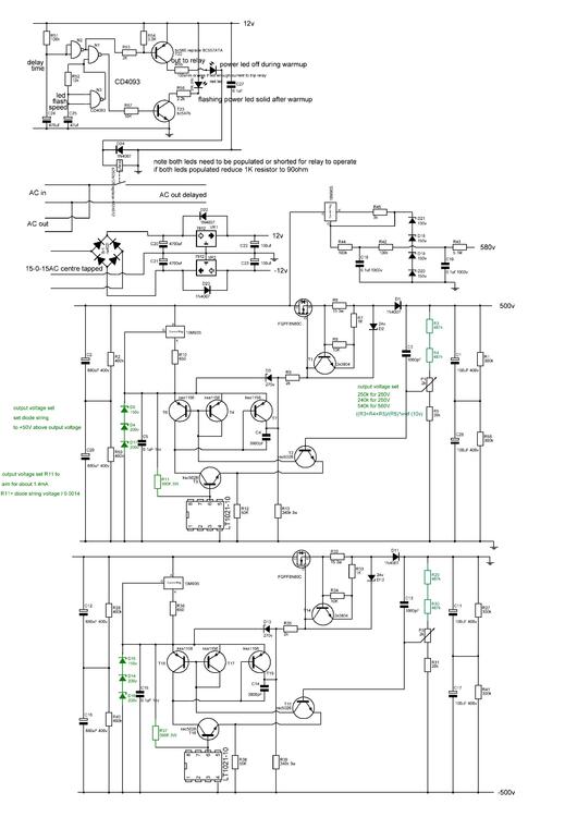
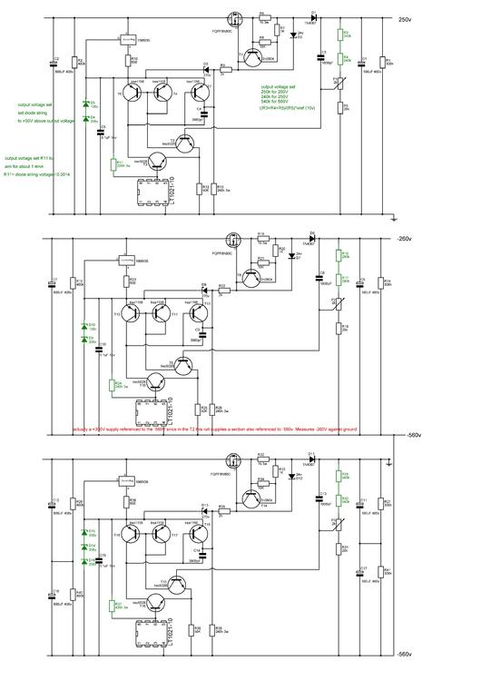
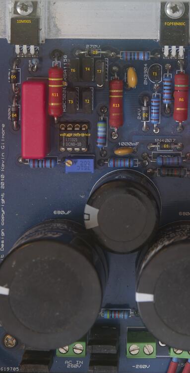
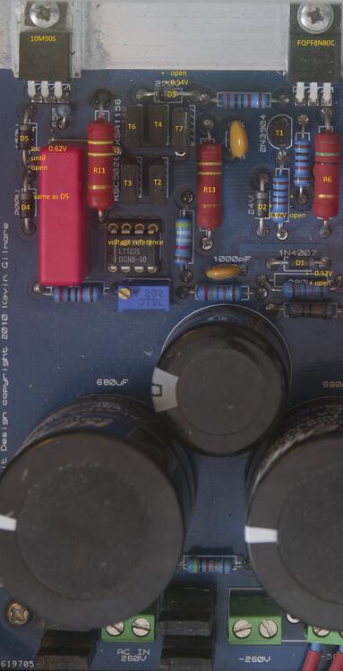
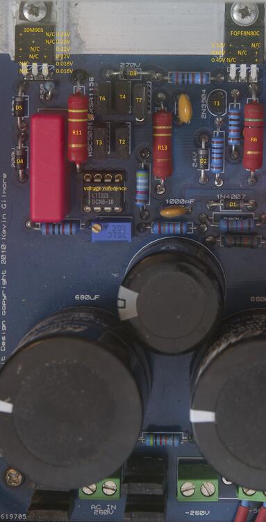
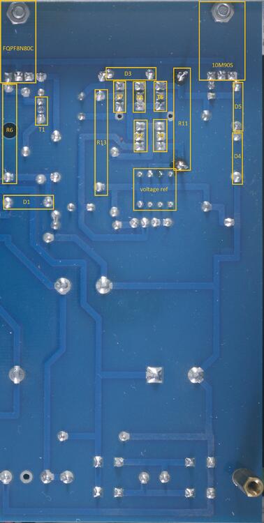
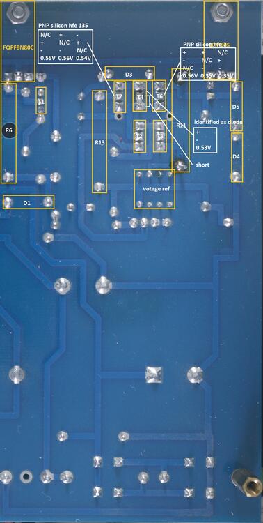
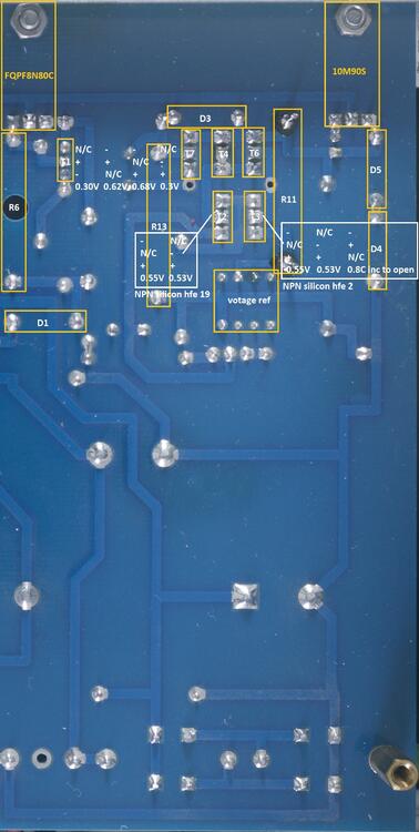
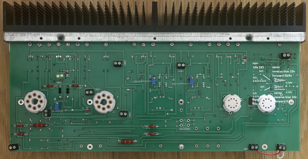
Since the T2 needs a complex power supply I am also including a T2 power supply testing guide. There are multiple options for the T2 power supply but the one I built is: The gerbers can be found here: <insert link> The guide is intended for both pre-power on verification of an amp build, verification of voltages on power on and general troubleshooting. All tests are performed using a Brymen BM869s and peak DCA75. Using a different multimeter may effect the results slightly but you should still get similar behaviours and ball-park figures. All tests are performed with the psu not connected to an amp and no mains transformer connected. unfortunately many of the transistors are packed tightly together so it is not easy or really possible to get test probes onto all the legs of all the transistors from the top and so the verification guide will be separated into two halves: testing from the top and testing from the bottom. Since all the high voltage power supplies are basically identical except for differing values for some resistors ad the pre regulator zeners I will cover one psu rai and the diode tests and dca75 tests should be the same for the other high voltage rails. (The 500V and above rails also have two caps in series with bleed resistors in parallel for the input smoothing and output smoothing to reduce the financial cost of the caps and increase the cap options) The low voltage rails are trivial - diode bridge, bulk cap, monolithic off the shelf regulator and smoothing cap and so will not be covered. NOTE the 3w resistor which direct connects to the 10 volt reference will get hot (depending upon the supply rail) it can reach 80C+, If you look at my schematics above I suggest increasing the value of the resistor to reduce the current and decrease the temperature. Also raise it from the pcb as much as possible to keep it away from the nearby 0.1uF capacitor. NOTE if you use 0.1% precision resistors for the output voltage set resistors then they must be rated at above 250V for the 560V rail or (in my experience if you use 250V rated working voltage resistors their resistance will drift higher and higher with time and the 560V rail will eventually hit the zener string voltage of 600V and this will cause an uncorrectable dc offset in your T2 amp). Transistor and diode location Top The two ksc5026 (T3 and T2) form a long tail pair with T3 input being the 10V reference and T2 input being the the voltage across R5 (and half of P1) in the voltage set string. To improve the performance of the differential amp T6 and T4 form a current mirror. R12 is the common resistor for the long tail. The output of the long tail comes from the collector of T3 and goes to T7. Probe Tests from above Diode test of the zener pre regulator D5 and D4 measuring across each separately, you will get about 0.6V drop, probes reversed the multimeter will register a steadily increasing voltage until it shows open. This is true of each zener in the string. Diode test D2 you will get about 0.6v drop in one direction and an instant open in the other Diode test D1 you will get about 0.52v drop in one direction and an instant open in the other Diode test D3 you will get about 0.54v drop in one direction and an instant open in the other Note it is possible for a transistor to fail in such a way it has very little gain but still has a diode drop and so diode checking transistors is not a foolproof measure of a transistors health. But 0V drop when not expected indicates a short etc. Diode and dca75 tests of the 10m90s NOTE the 10m90s has a live tab and absolutely must be insulated from the heatsink it is mounted to. Like the 10m90s in the t2 amp boards the 10m90s measures the same when the polarity of the probes has been reversed. Just like the T2 amp the peak dca75 can't identify this component in circuit and variously shows it as a low voltage zener ~ 1.6V or an led. Diode and dca75 tests of the fqp8n80s The peak dca75 can't identify this component in circuit and variously misidentifies it as two diodes or a diode and led. Diode checks from underside Transistor and diode location Bottom Diode test T1 2N3904 NPN transistor. forms the active part of the current limit circuit. It monitors the current through R15 and when the voltage drop across the resistor gets too high T1 starts to cut off the pass mosfet FQPF8M80C. If you get correct voltage output with no load but any load massively decreases the output down to about 75V suspect T1 has gone short circuit. Diode and DCA 75 test T2 and T3 KSC5026 NPN transistor. These form the long tail pair differential amp which compares the voltage reference against a portion of the output voltage controlled by the trimmer P1 and the series resistor ladder R3, R4 R5. There should be very close to 10V across R5 if not one possibility is R3 and R4 have too higher a resistance value, possibility from using resistors with a too low working voltage - especially in the -560V rail which puts more than 250V across each of R3 and R4 in the series ladder. NOTE T2 is connected to a both ends of a cap and so this cap will slowly charge resulting in the diode test reading showing an increasing voltage drop until the multimeter finally displays open when the cap has charged to the same voltage as the meter outputs and so no current flows at all fooling the meter into thinking there is an open circuit. This does not occur with T3 The dca75 reliably and correctly identifies T2 as a NPN silicon transistor hfe 19 and T3 as a NPN silicon transistor hfe 2. Diode and DCA75 test T4, T6 T7. Ksa156 PNP transistor. T4 and T6 form the current mirror for the long pair differential amp. NOTE T4 has base and collector shorted together and so measures similarly to a single diode. The DCA correctly and reliably identifies T7 as a PNP transistor hfe 135 The DCA obviously identifies T4 as a diode junction if you don't connect the 3rd lead, otherwise it just reports a short between two of the leads - which is correct. The DCA correctly and reliably identifies T6 as a PNP transistor hfe 2 <<<work in progress>>>1 point
-
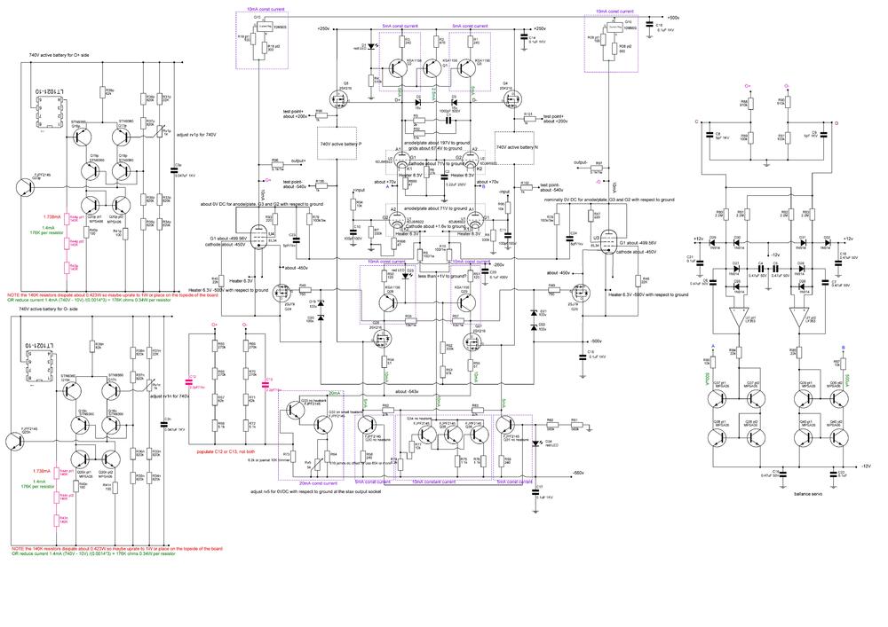
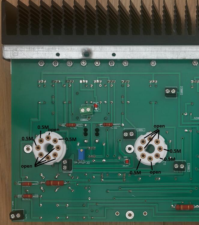
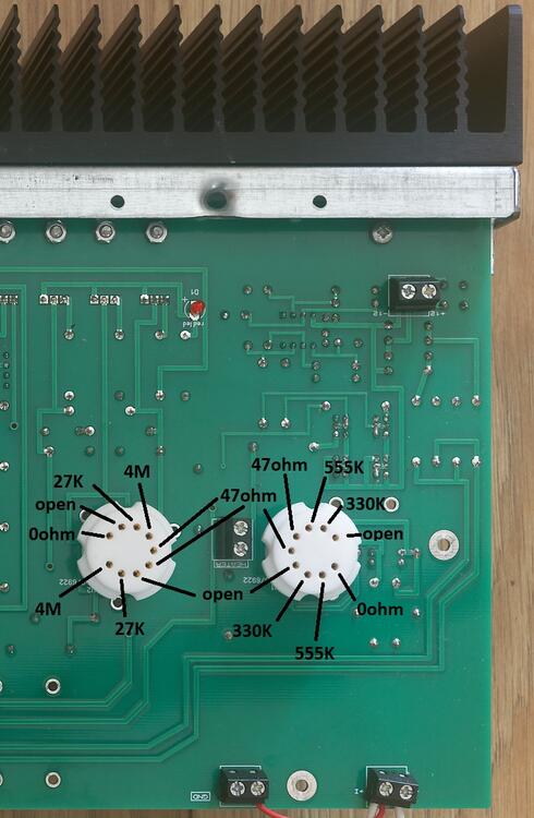
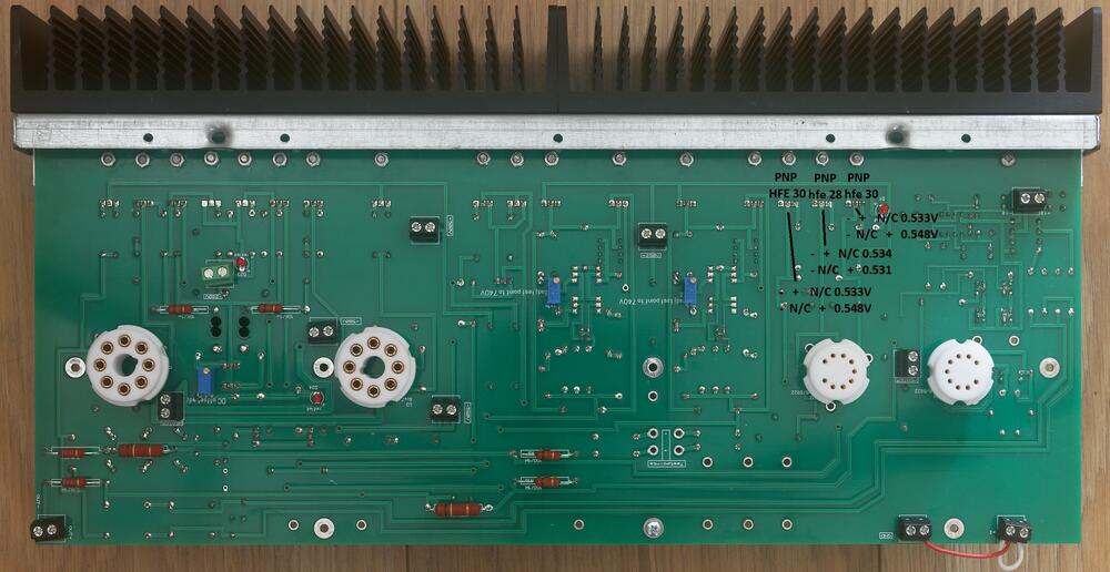
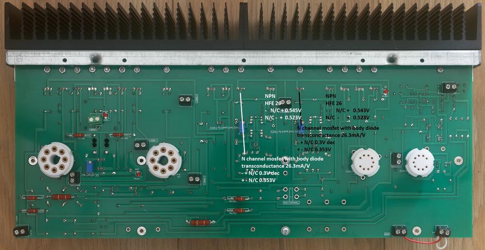
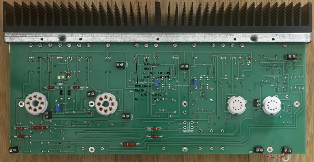
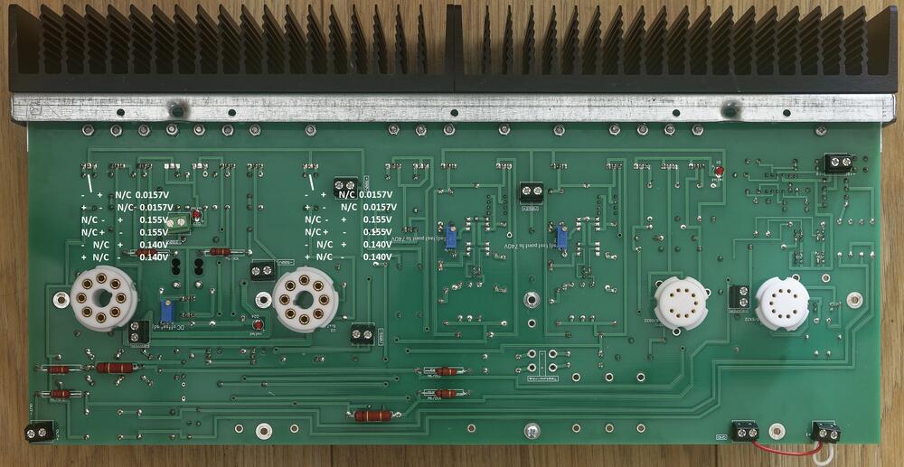
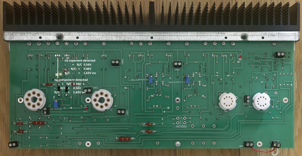
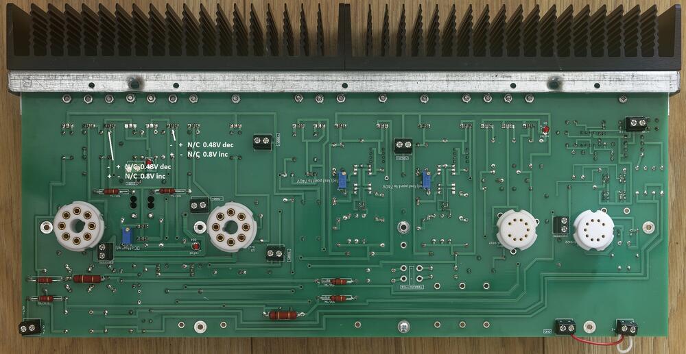
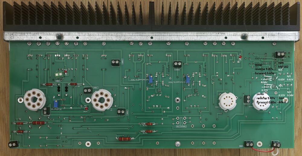
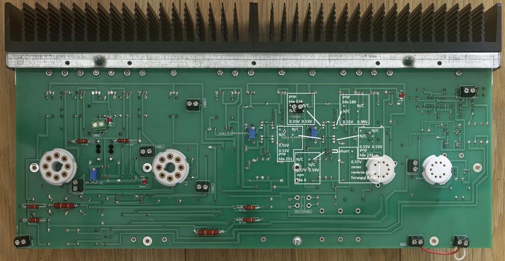
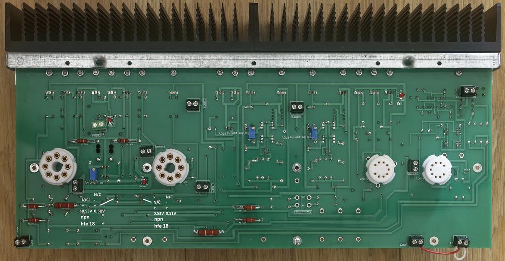
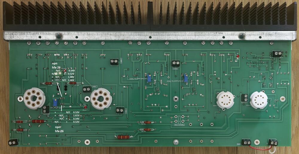
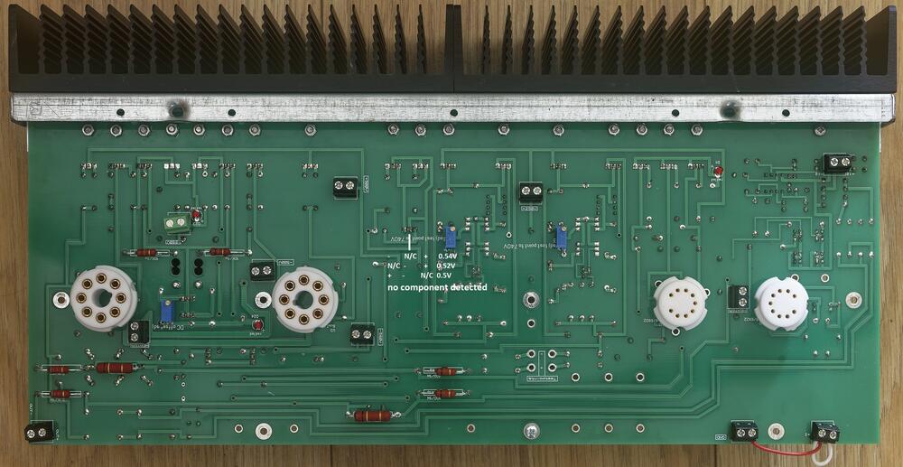
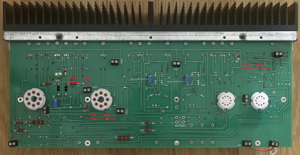
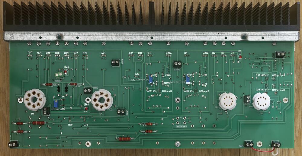
The unofficial mostly modern T2 troubleshooting and verification guide. Weclome, this guide covers the mostly modern T2 which has the following schematic: The gerbers for the amp can be found here: https://drive.google.com/drive/folders/1r3g2TAtBUaBdiMorTWX7yYgeJ7maQbYW and the gerbers are staxt2nc3fdh7.zip The guide is intended for both pre-power on verification of an amp build, verification of voltages on power on and general troubleshooting. All tests are performed using a Brymen BM869s and peak DCA75. Using a different multimeter may effect the results slightly but you should still get similar behaviours and ball-park figures. Transistor and Diode Location Section 1. Build verification with no valves installed and no wires/volume control connected to the amp All of these checks can be performed with a multimeter from the top side of the amp board leds Checks. All 3 leds on each channel should read about 0.55V voltage drop in forward bias (multimeter + terminal/red lead connected to led + and multimeter - terminal black lead connected to led -) and open circuit in reverse bias (swap the probes around) when tested with a multimeter in diode check mode. The leds will not light from the diode test due t the current draw if the components around them. The exact forward voltage drop will depend upon the characteristics of the red led but anything significantly different here indicates a problem. 0 voltage drop in both directions indicates a short across the led or the components it connected to. check for solder bridges and failed short transistors. 0L indicates in both directions means the led has dry solder joints or is blown. using a multimeter in resistance mode check the leds D23 close to the -360VDC psu input. In forward bias expect around 4M ohms. With the probes reversed you should get open circuit. D24 is the led closest to the octal socket for the EL34 and should read about 1.8M in forward bias and about 1.9M in reverse. D1 is between in the 9 pin sockets but close to the heatsinks. This should read about 1.5M in both directions. Readings in both directions of a few hundred K ohms or lower indicate the led may have been leaky or a transistor it is connected to has gone short circuit or a solder bridge. Input terminal checks With the multimeter in resistance mode and the - terminal connected to the amp ground, and the positive terminal connected to the + input of the amp you should get about 340K and the same for the - input. Naturally expect the same results for the other channel. If significantly different suspect incorrect resistors for R94, R7 (positive input). Or R95, R8 on the - input. Output terminal checks With the multimeter in resistance mode and the - terminal connected to the amp ground, and the positive terminal connected to the + output of the amp you should get about 0.5M and the same for the - output. Naturally expect the same results for the other channel. Valve Socket Checks. With the multimeter in resistance mode and the - terminal connected to the amp ground, and the positive terminal expect the following resistances for both EL34s: (socket viewed from the top of the amp). (note the 0.5M reading may start lower and quickly ram up and the small capacitors in the circuit are charged by the multimeter). For the 6922s (socket viewed from the top of the amp) Diode Checks of transistors Note it is possible for a transistor to fail in such a way it has very little gain but still has a diode drop and so diode checking transistors is not a foolproof measure of a transistors health. But 0V drop when not expected indicates a short etc. Diode checks KSA1156 checks Q1, Q2, Q3 two of the ksa1156s (Q2 and A3) measure the same in diode mode the centre one (Q1) differs slightly. All combinations of probes and pins on a transistor result in open circuit unless otherwise shown otherwise: + indicates positive multimeter probe attached, - indicates negative multimeter probe attached n/c indicates no probe attachment. Note: for the other channel EACH KSA1156 is rotated 180 degrees about the y (vertical) axis. Peak DCA in circuit testing Q1-3 The peak DCA 75 identifies all 3 transistors as PNP silicon. The centre with a hfe or around 28 and the other two with slightly higher hfe of 30 to 31. This test is reliable, anything significantly different indicates a problem. Note it is easier to do these tests from the underside although you can hook up the dca proe hooks to something like a sensepeek weighted self standing spring loaded probe tip assembly and test easily from the top (https://sensepeek.com/pcbite-20 Diode check and Peak DCA 75 for Q23P FJPF2145 This is reliably identified as a NPN with hfe 26 and is part of the virtual battery connected to the + output side of the channel. NOTE: It has a mirror image pinout compared to the ksa1156s. Diode check and peak DCA 75 check for Q5 2SK216 This is reliably identified as a N channel mosfet with body diode and has a transconductance of 23.3mA/V. Although not part of the virtual battery it is directly connected to it. WANRING This transistor has a live mounting tab and must be fully insulated from the heatsink. A resistance check from the metal tab to the heatsink it is mounted on absolutely must read open circuit. Diode measurement for this transistor does not show a stable reading. In this case dec indicates a reading that decreases over time. The next two transistors in the heatsink row are Q23N and Q4 which perform exactly the same role and are exactly the same type of transistors as Q23P and Q5 respectively and should measure about the same I got 28mA/V for the Q4 so expect a little variance here). NOTE: on the other channel the order of the 2SK216 and FJPF2145 are reversed. Diode check and peak DCA 75 check for Q35 and Q36 FJPF2145 These are the current providers (driven by Q34) for a 10mA constant current source that feeds the input 6922s. The job is equally divided between them and they should measure the same. The DCA75 reliably identifies them as NPN silicon hfe 25-26 Diode check and peak DCA 75 check for Q15 and Q10 (10M90S) These are identified out of circuit by the dca75 as N channel depletion mosfets. However, in this circuit they provide anode current and are wired in such a way the DCA75 can not identify them and reports no component. The DCA75 should not report any shorts and the metal mounting tab is live and absolutely must be insulated from the heatsink they are mounted on. Q15 and Q10 are identically configured and should measure the same. The gate and cathodes are connected together with resistors totalling only 400ohms so the diode drop voltages will be lower than for the other transistors also unlike the other transistors all combination of probes will result in a voltage drop. The voltage drop should be the same in the forward and reverse directions. Diode check and peak DCA 75 check for Q28 and Q29 (KSA1156) These are identified out of circuit by the dca75 as PNP silicon. However in this circuit they are wired in such a way the DCA75 can not identify them and reports no component. Each should measure the same. Diode check and peak DCA 75 check for Q26 and Q27 (2SK216) These transistors do not produce stable diode voltage drops. Diode check and peak DCA 75 check for Q25 and Q24 (2SJ79) These transistors are not easy to get a stable reading on. Diode and peak dca75 Check Balance servo Q37 - Q40 (MPSA06) 4 of the MPSA06es have their collectors and bases shorted together and so can be considered to only have two pins as far as diode checking concerned. NOTE for any transistor with shorted pins only two dca75 probes were used (one to the shorted pins and the other to the non shorted pin) to avoid the dca just reporting probes shorted. Understandably ni this case the dca75 can not identify the component as a transistor and instead reports a 9.87V zener. All other transistors are correctly identified and hfe provided. Diode and peak dca75 Check Virtual Battery Q16 - Q18 (STN9360) and Q20 (MPSA06) the other virtual battery in the channel (just to the left) should measure similarly and is identically laid out. Q20 pt 1 has collector and base shorted. All 4 stn9360 should diode measure similarly. NOTE for any transistor with shorted pins only two dca75 probes were used (one to the shorted pins and the other to the non shorted pin) to avoid the dca just reporting probes shorted. Understandably ni this case the dca75 can not identify the component as a transistor and instead reports a 10V zener. All other transistors are correctly identified and hfe provided. The stn9360 are pnp and the remaining non shorted mpsa06 as npn Diode and peak dca75 check Q30 and Q31 (FJPF2145) Each transistor provides a separate 5mA current source and are directly connected to the virtual battery. With the led D24 across their base and emitter. Each is identically configured and should read the same. Dca75 reliably identifies both transistors as npn both hfe 18 Diode and peak dca75 check Q32 (on seperate small heatsink) and Q33 (FJPF2145) this forms a 20mA current source which is controlled by Rv5 and sets the DC offset. DCA75 reliably identifies both transistors as npn both with hfe 26 Diode and peak dca75 check Q34 (FJPF2145) Q34 provides control for Q35 and Q36 which creates a 10mA current source. The dca75 says no component detected. <<< IN PROGRESS >>> #include <usual_disclaimer.h> #include <usual_high voltage_warnings.h>1 point
-
update on the RIP T2. The four 270K resistors R65 to R68 are discoloured I believe because of the higher than expected DC voltages across them from the massive DC imbalance. Otherwise there are no visible signs of problems. I found a dead 2SK216 in addition to the dead 2SJ79 on the same channel that the 6922 failed on. Diode testing found the dead J79 but to find the dead K216 I used my peak dca75 to measure the two ksa1156s and found radically different hfe measurements (43 vs 143) so I removed the other J79 and the readings were dd not change. The removed J79 measured ok. So I suspected the K216es and removed them 216es one measured good and one bad. The good K216 was connected to the bad J79 and good J79 connected to the bad K216... The ksa1156es measured the same hfe when the 4 transistors were removed so I believe they are ok. I'm replacing all 4 mosfets with ksa1220A and KSC2690A because that's all I have... The other channel had the same imbalance issues and one of the K216es there is dead too. Both channels now have 1220 and 2690a installed. But I noticed that the ksa1156s on the channel with the failed 6922 measured hfe 51 in circuit and the channel with only the single failed k216 the same ksa1156s measured 2hfe. Hmm... looking at the circuit I decided to measure the resistance across led between the emitter and base of the ksa1156es... channel with the failed 6922 about 150K and about 190K leads revered. Channel with single bad k216 about 3.4M and open when reverse biased... So either the led or the ksa1156s where leaking. Desoldered the ksa1156s and tested them... ok. desoldered the D23 led and replaced it. Now 3.4M and open circuit. So the led had gone leaky. At least both channels now measure the same... The other led close to the EL34 (D24 ) on the channel with the dead 6922 is also leaky . So score so far: right channel 6922 shorted heater to cathode K216 DCA75 measures it as a zener diode J79 DCA75 measures it as two diodes Led Brymen bm869s measures it as a 150K resistor Led Brymen bm869s measures it as a 88K resistor Left channel K216 DCA75 measures it as zener diode1 point


